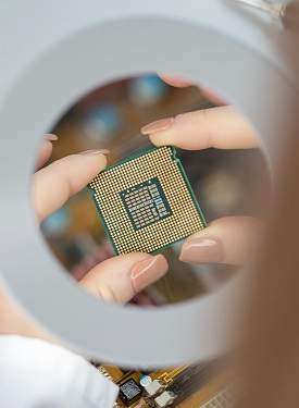

AMD (Advanced Micro Devices) is an American multinational semiconductor unit company that develops computer processors & related technologies for business and consumer markets. The company’s key products contain motherboard chipsets, microprocessors, embedded processors, and graphics processors for workstations, servers, personal computers & embedded system applications.
AMD is inventing its x86 hybrid processor technology articulated along the Arm big.LITTLE hybrid CPU core. Under this, the processor has two types of CPU cores with very dissimilar performance/Watt band that emphasizes performance and remains inactive under mild processing work-loads. In contrast, the other hand manages most frivolous processing loads that do not need powerful cores.
What is a Hybrid x86 CPU?
Based on the latest technology, it is a microchip designed by Intel. This minute 12×12 package is constructed using Intel’s favorite technology. A 22FFL IO chip connected with TSVs (Tab Separated Values) to a 10nm die both a sole Sunny Cove core & four Atom cores. This small chip is slighter than a dime and is intended to have 2-mW standby power. It is considered that this chip is made for mobile devices.
AMD files a Patent
AMD has submitted a patent telling of a method for dealing out work-loads to be swapped between the two CPU core types and named it as best AMD CPU. Rendering to the patent, CPUs would trust core operation metrics to govern when it was suitable to move a load from one to another type of CPU. Planned metrics comprise the total of time the CPU has been at work at maximum speed. It also includes the sum of time the CPU has been using extreme memory, average use over an average time, and an overall category in which an assignment is progressed from one CPU to another depending on indefinite metrics connected to the accomplishment of the task.
When the CPU identifies that a work-load should transfer from CPU X to CPU Y, the core presently performing the work (CPU X, in this case) is placed into an idle or delayed state. The state of CPU X is protected to memory and laden by CPU Y, which keeps continuing the process. The patent defines these shifts as two-directional — the minor core can swing work to the big or vice-versa.
Unlike similar CPU core designs where load from one core is flawlessly picked up by an alternative over a target cache like the L3, there is roughly a logic elaborated in an exchange between the two core kinds. According to the patent submission, in an AMD hybrid computer, the two CPU core forms are interfaced over the processor’s chief switching fabric and not a target cache.
ARM vs. x86
ARM and x86 are two different things, and in this article, we are going to dig out all the differences between them. For context, x86 runs on most computers, while Arm is one on your mobile phones. The Arm is an acronym for advanced RISC (Reduced Instruction Set Computing) machines. A CPU is given specific instructions so that it can work accordingly. Powerful CPUs require very complex and unique instructions.
Today’s applications definitely cannot be written in CPU instructions as they will be too complex. Therefore, they are written in higher-level programming languages such as Java and C++. A more complex instruction set will suck more power, and a simple instruction set is present for power-efficient CPUs. This is the basic difference between an ARM and x86. Following are some more differences between them.
| ARM | x86 |
| Targets power efficiency | It targets peak performance |
| Mainly structured on RISC | Based on CISC (Complex Instruction Set Computing) |
| Less complex structures | Use more complex structures leading to better performance |
| Ideal for mobiles | Ideal for computers |
| More wide applications | Less wide applications comparatively |
Big.Little gained This Fight
Almost a decade ago, questions were asked to Intel’s smartphone SoC (System on a Chip) designers that why they were trusting DVFS (Dynamic Voltage and Frequency Scaling) to retain Atom’s power ingesting modest rather than Big. Little. Rendered to Intel’s architects, DVFS was inexpensive with what Big.Little might bring when one measured the silicon die space necessities & the overall power efficiency.
It may have been factual at the time. Medfield was usually good with the midrange Cortex-A9 gadgets as it was planned to compete against, but it doesn’t appear to be factual today. At the time, Medfield was constructed on the 32nm processor node, whereas the Cortex-A9 was usually built on 40nm or 28nm. Surprisingly, if we count conventionally, TSMC (Taiwan Semiconductor Manufacturing Company) & Intel have been over multiple complete node shrinks. Intel’s 10nm expertise is regarded as identical to TSMC’s 7nm node. The die magnitude drawback for the exploitation of a hybrid x86 core plan is lesser than it used to be.
The great question where AMD is worried is whether the firm will shape a new from the ground-up CPU core or if it will go back to a design similar to Jaguar & use that as a foundation for upcoming products. Only time will tell what AMD CPU update will offer to us.
Final Verdict
We are not expecting to see hybrid cores from top AMD CPUs in the year 2021, but we will see them anywhere from 2022 to 2023. Now that we see some of the power reserves the Apple M1 brings to its OS preparation, we assume both Intel & AMD to do work with Microsoft to approve similar tech. Hybrid cores will not do a lot much for x86 CPU power ingesting at full load/clock, but they might decrease power feasting significantly. We know that now Windows 11 Is forthcoming, and Alder Lake is making itself ready for the launch. No one has publicly proclaimed that this type of hybrid scheduler will do the work on Windows 11, but it’s almost guaranteed to be noticeable.